Home
News
Insurance
Lawyer
Beauty salon
Mastering Personal Finance in the U.S.: Budgeting, Saving, Credit & Investing
News
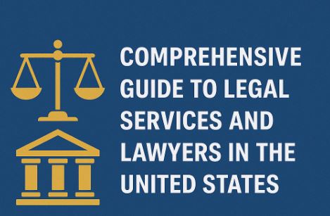
Comprehensive Guide to Legal Services and Lawyers in the United States
News
Top Insurance Companies in the U.S. & Insurance Models You Should Know
News
Top 5 Ways to Earn $2000 a Month from Home Without Special Skills
News
This U.S. City Will Pay You to Move There – Can You Believe It?
News
5 World-Famous Products That Were Invented... By Accident!
News
7 Unusual Jobs with Salaries Over $100,000 Per Year – You Won’t Believe #4!
News
This 10-Question Quiz Reveals Your Social Intelligence – Most People Fail #7
News
Are You Being Misled by These Everyday Deceptions?
News
20 Fascinating U.S. Secrets Most Americans Don't Know
News
80% Discount Vouchers for Online Shopping
News
What‘s the difference between Spa and Salon?
Beauty salon
What Factors Do Beauty Clients Use to Choose a Beauty Salon?
Beauty salon
6 of the Best Cosmetic Skin Treatments
Beauty salon
How Often Should You Get a Haircut?
Beauty salon
Tips on What To Look For in A Good Hair Stylist
Beauty salon
The Importance of Regular Salon Visits
Beauty salon
5 Steps To Prepare Your Hair For Color
Beauty salon
What You Need To Know About Your First Salon Visit
Beauty salon
How to Choose the Right Hair and Beauty Salon?
Beauty salon
Top 5 Types of Beauty Salons and Services
Beauty salon
Understanding Contingency Fees
Lawyer
Different types of lawyers for the most common legal problems
Lawyer
Criminal vs. Civil Law: Key Differences Between the Two
Lawyer
How to Prepare for an Initial Consultation With an Attorney
Lawyer
Most read news
Top 5 Types of Beauty Salons and Services
What‘s the difference between Spa and Salon?
Top Insurance Companies in the U.S. & Insurance Models You Should Know
6 of the Best Cosmetic Skin Treatments
First meeting with a lawyer
How can I lower my insurance premiums without losing coverage?
Home
News
Insurance
Lawyer
Beauty salon


.jpg)